Top 5 Printed Circuit Board Stack-Up Design Mistakes


Identifying Errors and Guidelines on How to Prevent Them

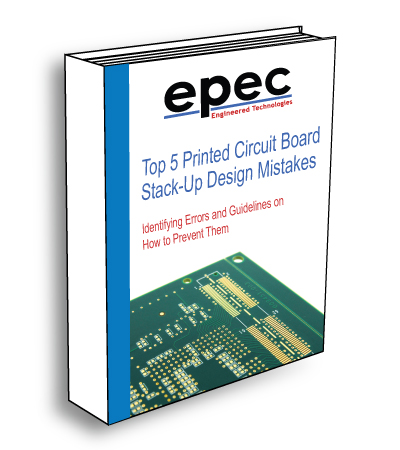
Inside the Top 5 Printed Circuit Board Stack-Up Design Mistakes Ebook, we will look at what to look for in terms of PCB stack-up design issues and provide guidance on how to mitigate each issue.

The stack-up is defined by the design team or by the manufacturing of the printed circuit board (PCB). All PCBs have a determined shape and size and an overall dimension X and Y. The PCB also has a predetermined overall allowed thickness to be met including a tolerance by manufacturing. The stack is more than copper weight, layer count, and overall thickness – it also defines dielectrics, material(s), and tolerance. From double-sided to multilayers, all PCBs have a stack-up to meet the overall thickness required. 
What’s Inside:

  • Mixed Copper Weight
  • Data Set Impacts on Stack-Up Details
  • Layer Count
  • And more…
Top 5 Printed Circuit Board Stack-Up Design Mistakes

As a printed circuit board manufacturer, we find that the stack is either defined, designed in, and very specific or suggested as layers and overall thickness and left up to us as the manufacturer to determine the stack.

Stack-ups in general are critical to a properly functioning PCB. In most cases, supplying the overall thickness of the printed circuit board (and if the part is to be RoHS compliant and the finished desired copper weight) is enough information for production to determine what materials and thickness to use for the stack.

Using Epec’s free DFM service for stack-up assistance at the design and layout stage can save you cost and time to production when you place your order.

Learn These 5 PCB Stack-Up Design Mistakes

Fill out our short form to receive your FREE copy!